Consortium
The NANOTHERM consortium (18 partners from 8 European States) is an interdisciplinary, highly profiled team of experts from packaging technology, foundries, chip manufacturers, optical companies and material suppliers. It is balanced and involves all the supply chain partners in order to anticipate the cost-effective introduction of these new technologies and future products on the market:
- 7 major European research institutes / universities addressing the fundamental scientific and technical issues
- 6 major industries playing the role of end-user directly addressing to automotive, solid state lighting, avionics, communication, chip manufacturing, packaging technology and material development,
- 5 SMEs providing specific technological capabilities during the project and expecting short time-to-market benefits as return on investments in the exploitation phase.
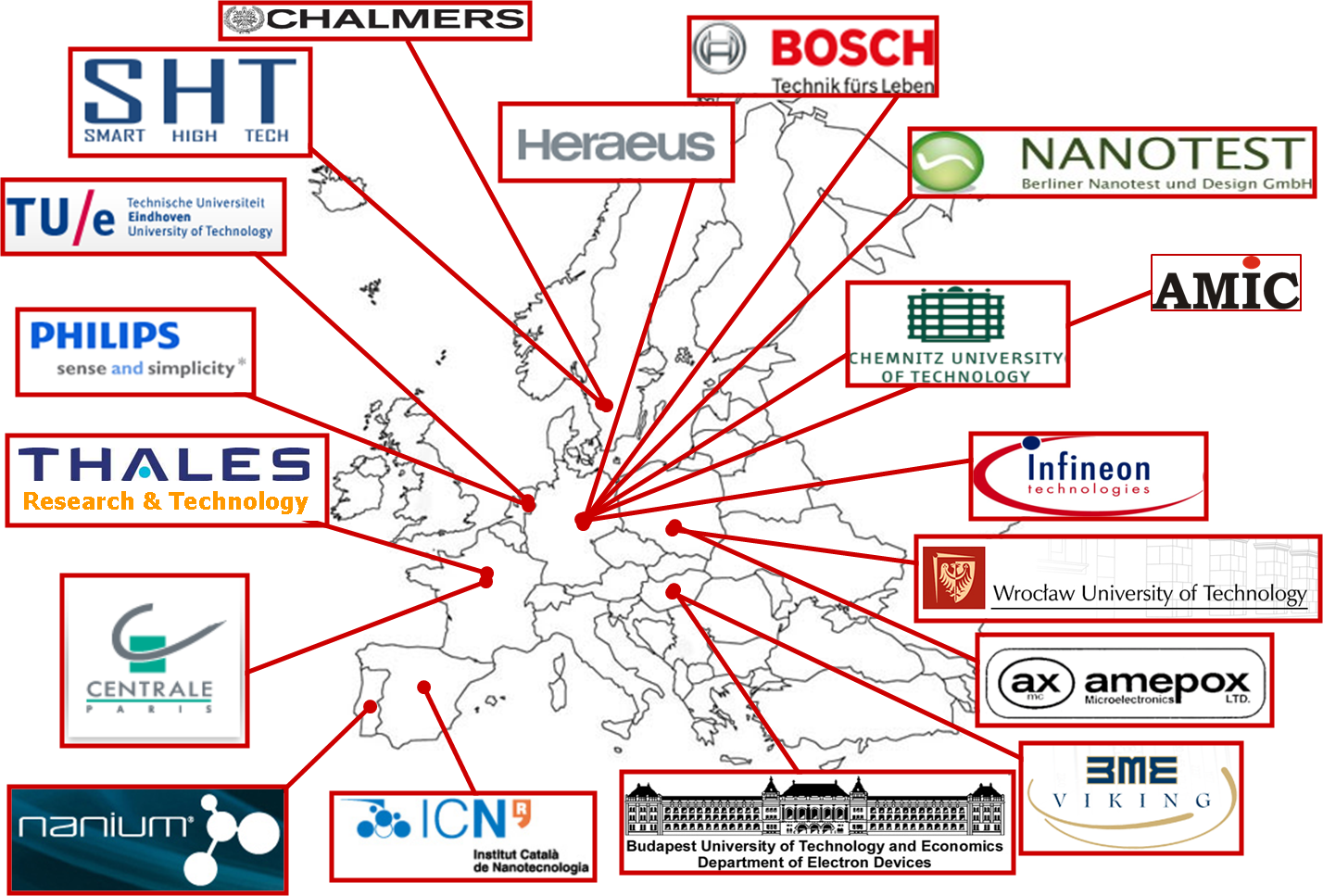
Partners Description: (link to individual description below)
- THALES Research & Technology
- Philips
- Bosch
- Heraeus
- Nanotest
- Technical University of Chemnitz
- Ecole Centrale Paris
- Smart High Tech AB
- Wroclaw University of Technology
- AMEPOX
- Budapest University of Technology and Economics
- CHALMERS university of technology
- AMIC Angewandte Micro-Messtechnik GmbH
- NANIUM
- Infineon technologies
- Eindhoven University of Technology
- BME VIKING
- Catalan Institute of Nanotechnology
THALES Research & Technology
THALES (formerly THOMSON-CSF) Research and Technology - France located near Paris, is the main multidisciplinary research unit of the THALES group, one of the major world players in civilian & professional electronics. Through its internal activities and scientific links with industries and universities, either in France or internationally, TRT is participating in the preparation of THALES industrial future in strategic R&D fields. In addition to R&D activities, TRT also provides scientific and technical advice, expertise or services for the company. TRT has been participating in or leading numerous research programs, either national or EU-funded, in the frame of ACTS, TELEMATICS, ESPRIT, BRITE-EURAM, TMR, ISM programme Its technological lead in these high-added-value fields naturally is compounded with the best production solution at the lowest cost. Owing to its production capacities and to its organizational flexibility, THALES Research & Technology ranks among top competitors worldwide. Technological expertise and extensive know-how make THALES Research & Technology a privileged partner for developing top-performance and highly competitive products and systems.
With over 250 highly skilled staff, 13000 m² of labs of which 1700 m² clean rooms, TRT research teams perform pioneering work in the most advanced areas of optics & opto-electronics, electronic components for microwave applications, advanced interconnect and packaging, Micro-systems for acoustic, RF & optic applications, materials, software architecture and cognitive science. S&T skills, ranging from materials elaboration (epitaxy of various semiconductors or magnetic thin films, ceramics, polymers, PZT), through component modeling, processing, testing, assembly and packaging, to integration in appropriate demonstrators are available on site and allow full validation of the technologies investigated before their transfer to operational divisions of the THALES Group, including the Business Group Communication Components (Turnover: 945 Meuro in 2000) which proposes RF and millimeter wave components and modules for the telecommunication civilian market.
Philips
Royal Philips Electronics of the Netherlands is a global leader in healthcare, lifestyle and lighting, delivering products, services and solutions through the brand promise of "sense and simplicity". Headquartered in the Netherlands, Philips employs approximately 121,400 employees in more than 60 countries worldwide. With sales of EUR 26 billion in 2008, the company is a market leader in medical diagnostic imaging and patient monitoring systems, energy efficient lighting solutions, personal care and home appliances, as well as consumer electronics. In 2008, Philips spent EUR 1.6 billion on R&D and holds 80,000 registered patents, which shows the innovative nature of the company. In a world in which technology increasingly touches every aspect of daily life, we want to bring 'sense and simplicity' to consumers with advanced, easy to use products that are designed specifically to meet their needs, wherever in the world they may be.
Philips Research was founded in 1914 in Eindhoven, The Netherlands, as part of Royal Philips Electronics. Philips Research is one of the world’s major private research organizations, staffed by around 2,100 people. Its activities have led to the award of some 100,000 patent and design rights, and the publishing of many thousands of technical and scientific papers. In close cooperation with the Philips Product Divisions, the Philips Research organization generates options for new and improved products and processes and produces important patents in many fields. Positioned at the front-end of the innovation process, we work on everything from spotting trends and ideation to proof of concept and – where needed – first-of-a-kind product development. In order to fulfill our ambition, it is crucial that we work together with companies that are complementary to Philips and share our vision. Philips Research, as one of the pioneers of open innovation, is actively leveraging its deep competences, know-how and IP to work with selected companies and organizations with the purpose of creating win-win propositions. For almost a century, our approach has enabled us to surprise people with breakthrough innovations – everything from lamps, radios and televisions to medical equipment, electric shavers and semiconductors. Along the way, we've been responsible for some truly ground-breaking discoveries and standards, such as the Rotalix X-ray tube, the high-pressure mercury lamp, the triple-headed dry electric razor, the Compact Cassette, and more recent innovations like the Brilliance 40 slice CT scanner, CD, DVD, and Ambilight TV.
The first involved department in the project is Product and Process Modelling which is the largest Virtual Prototyping group within Philips and has a well-established expertise in thermal and thermo-mechanical prediction and optimization of micro-electronic systems, fracture mechanics, multi-scale methods, non-linear finite element simulations and Physics-of-Failure based methods. The second involved department is Electronic Packaging and Thin Film which concentrates on Advanced packaging, electrical interconnect and assembly technologies, thin film technology, reliability and failure mechanics and advanced packaging industrialization. Example of application areas are solid state lighting, micro devices for minimal invasive healthcare, devices for healthcare imaging system and (micro) devices for consumer lifestyle applications. In addition to the above-mentioned capabilities of the departments, state of the art thin film processing and packaging capabilities, experimental characterization and (failure mode) test facilities are available.
Bosch
With sales of € 47.3 billion in 2010, Bosch is one of Germany’s largest industrial enterprises with a strong international focus. The group employs over 280,000 associates in the areas of automotive technology (59% of sales), industrial technology (14% of sales) as well as consumer goods and building technology (27% of sales). Ninety-two percent of the share capital is held by Robert Bosch Stiftung GmbH, a charitable foundation.
In the field of research and development with over 30,000 associates, Bosch’s expenditure totals 8,1 % of sales. In 2010 we applied over 3,800 patents for inventions worldwide. At Bosch, the way we do business is in tune with environmental protection. Bosch is determined to enhance the quality of life of people all around the world with solutions that are both innovative and beneficial.
“Reliability, credibility and legality are the essential factors for the business success of the Bosch Group.” (Hermann Scholl, Chairman of the Supervisory Board)
Corporate Research Division
The Corporate Sector Research and Advanced Engineering (CR) is responsible for the development of new technologies and product innovation in areas such as automotive electronics, energy and body systems, safety and security systems, very large scale integration, and manufacturing techniques. Research labs are located in Germany, Switzerland and the USA. Experts in this well as other divisions participate actively in standardization bodies and expert groups.
The department CR/APP of the Corporate Research Division develops polymer materials and processing techniques that are relevant to all units within the Robert Bosch Group. Initiation of Pilot-Projects for innovative products and their transfer to Bosch Business Units are the main activities. For building up demonstrators, investigating on assembly processes, characterizing materials and running tests, Bosch has numerous equipment for electronic packaging in clean room, (die attach, dispensing and screen printing equipment) and different departments, which will contribute to the project such as testing of high current applications and application tests under automotive conditions.
Heraeus
Heraeus is a globally active precious metals and technology Group with firm roots in Germany. The company has been family-owned for 160 years. The areas of expertise of Heraeus Materials Technology GmbH and Co. KG encompass the manufacturing of precious metals and highly sophisticated materials like gold, silver, platinum, special metals and special alloys. The company develops and produces numerous special substrates and materials for electronics assembly like precious metals powders, SMT adhesives, conductive adhesives, solder powders and solder pastes. Heraeus is a supplier of high quality materials for assembly in power electronics like Pb-free solder pastes, silver conductive adhesives and silver sinter pastes for pressure sintering and special substrates. These products are well established in the market.
The current development objectives of Heraeus relate, amongst others, to increasing the reliability and the efficiency of microelectronics systems, especially those used at high operation temperatures. The research and development potential allows a fast and flexible development followed by mass production manufacturing of new materials in power electronics.
As a technology based company and supplier of assembly materials, Heraeus has participated to the planning and realization of numerous projects funded by the German Ministry of Research and Industry like Innolot, Flexjet, NanoFlux, ThermoFlux, UltiMo, HotPowCon, HI-LEVEL and ProPower. As technology leader in assembly materials for the electronics industry, Heraeus employs highly skilled and specialized R&D scientists and technicians, and is equipped with R&D facilities for material design and development as well as sample making in small to medium quantity. This includes:
- adhesive making equipment (mixers, dispergation equipments, packing)
- adhesive processing equipment (printing, dispensing, die placing, curing)
- adhesive characterization equipment (testing of rheology, electrical resistance, thermal conductivity, adhesion, ageing, metallography, optical and electronic microscopy)
- substrate making equipment (stamping, laminating, electroplating)
- substrate characterization equipment (testing of geometry, surface properties)
Nanotest
Berliner Nanotest und Design GmbH serves as a full-scale provider of engineering services for reliability in microsystem technologies and nanotechnology, for micro-testing and micro-analyses.
Nanotest spun off from the Fraunhofer Micro Materials Center in 2004. There from, far reaching experiences in the field of reliability testing and material properties determination are available.
Specific Profile and Expertise: The main activities of Nanotest are in development, services, costumer- specific equipment, research and consulting in the field of micro- and nanomaterials compounds and micro- and nanoreliability for high tech applications in various fields, e.g. automotive electronics and security applications.
Main areas of expertise include:
- reliability analyses of microcomponents for MEMS, microsystems and micro-/nanomaterials for a variety of applications using advanced experimental tools
- simulation of micro- and nano-stacks and packages by FEM and other techniques or tools
- thermal characterization of micro/nano materials and compounds
- evaluation of materials and component part combinations for packages by means of a combination of instruments, such as numerical simulation, experimental testing and other analysis methods (e.g. concerning reliability, lifetime, or optimum application mode). In FP 7, Nanotest was involved in the “NanoPack” project where he is in charge for development and performance of characterization of nanoscaled thermal interface materials
- TIM characterization: Platform for characterization of thermal interface materials using different modules e.g. for characterization of standard TIMs, characterization of highly conductive TIMs, characterization of very thin TIM-layer and characterization of aging behavior of TIMs.
- Calibration: Special techniques for precise calibration of different type of temperature sensors
- LED characterization: Thermo electrical characterization methods for LEDs
Technical University of Chemnitz
TUC department and chair “Materials and Reliability of Microsystems” was established recently. It focuses on material, technological as well as reliability aspects of micro-electronic systems and MEMS. The group has a longstanding experience in studies on thermal management and reliability in microsystem technology by both simulation (Molecular Dynamics and Finite Element Method) and experiments (materials testing, micro- and nano-analytical methods) on bulk, interface level and system level. The combination of numerical simulation with experimental methods is one focus of the activities. Joint projects and contracts with partners of the industry for research with regard to reliability of products and technologies are the main focus of the research. In the group exists a wide experience concerning lifetime modelling for different interconnect technologies and most difficult stress problems related to effects in microelectronics and microsystems technology. Project relevant facilities are thermal and mechanical modelling tools and various tools for the characterization of micro-materials like DSC, TGA, TMA and DMA. A wide experience concerning failure analysis, based on analytical tools like SAM, SEM and FIB is also present. Based on theoretical modelling on the basis of micro- and nano-materials characterization and supported by failure analysis, understanding, prediction and optimization of microsystems from a heat-transfer and mechanical reliability standpoint is the key role in the project.
Ecole Centrale Paris
The EM2C Laboratory (Laboratoire Energétique Moléculaire et Macroscopique, Combustion, CNRS UPR 288) is a CNRS laboratory hosted by the Ecole Centrale Paris (ECP) involving 30 researchers working in the fields of combustion, plasma and heat transfer (http://www.em2c.ecp.fr/). The Nano team has an established expertise in the micro and nanoscale modelling of heat transfer and also in the field of scanning thermal microscopy.
Smart High Tech AB
SHT was found in 2001, and located in Gothenburg, Sweden. For several years SHT has been focusing on the development of nanotechnology based electronics packaging materials and processes. Several new packaging materials and processes have been developed, such as Nano-TIM, nanotechnology enhanced conductive adhesive and carbon nanotube based packaging processes.
SHT has been involving in several national and EU-funded programs. Until now SHT has three patents related to Nano-TIM materials. SHT has been working as supplier to large mobile communication industries, and it has also built up its own intellectual property portfolio around design, materials fabrication and manufacturing technology for electronics applications.
Main areas of expertise include:
- Develop and provide unique nano-fiber based metal thermal interface materials with strength and mechanical performance through the polymer fiber network and excellent thermal performance through all-metal high thermally conductive pathways from surface to surface.
- Electrically and thermally conductive adhesives granting desirable electrical and mechanical benefits for surface mount applications and die attach.
- Integrating the well aligned carbon nanotubes (CNTs) into future packaging technologies.
SHT has its site at Physics building, Chalmers University of Technology. It has signed a long term contract with MC2 at Chalmers houses the Nanofabrication Laboratory, a world-class university cleanroom for research and fabrication of micro and nanotechnology. The Laboratory is a state-of-the art facility with 1240 m2 of cleanroom classified area with process and measurement tools providing a broad platform for the development and testing of new ideas in micro and nano technology. Besides, it has its own laboratory for assembly and reliability testing.
Wroclaw University of Technology
Politechnika Wroclawska (Wroclaw University of Technology, WrUT) is one of the biggest universities in Poland. It employs about 2000 university teachers and performs lectures for more than 32 000 students. The whole university consists of 12 faculties - two of them are connected with electronics.
The Laboratory for Interconnecting and Packaging Electronic Circuits (LIPEC) is the part of the Faculty of Microsystems Electronics and Photonics. The Faculty employs about 60 academic teachers, including 11 full professors. LIPEC was established in 1994. Its main research activity consists of following areas:
- Reliability in microelectronic packaging
- Designing and prototyping computer-controlled measurement systems for reliability tests
- Solder and adhesive joints reliability in Surface Mount Technology (SMT) - numerical prediction and testing
- Numerical prototyping of microelectronic components and micro-system packages
- Nanocomposites and electrically conductive microstructures for printed electronics
- Thermally conductive composites with nano- and micro-fillers
- Heat transfer modeling in molecular- and bulk-scale domain
- Electrically conductive adhesives (especially for microwave applications)
- Quality assessment of printed circuits boards (PCBs), solder and adhesives joints
- Technology for electronic devices manufacturing - design and optimization
- Packaging and recycling of materials oriented to green electronics
LIPEC has been involved in many European research projects in the frame of 5FP, 6EP, Eureka, Euripies, Eniac and collaborates with many research institutions in Europe (e.g. the Fraunhofer Institute for Electronic Nano Systems ENAS in Chemnitz).
Equipment for mechanical characterization and reliability tests:
ñ Climatic chamber (Challenge 250 Angelantonioni Industrie S.p.A.)
ñ Vibration exciter (LDS V406 Ling Dynamic System)
ñ Nanofocus X-ray inspection system & Computed Tomography (Phoenix Nanome|x 180, resolution: 0.4µm/voxel)
ñ Optical polarization microscope with digital image acquisition and processing (ZEISS Axio Imager 2 + AxioVision software)
ñ Automatic adhesion tester (PosiTest AT-A)
ñ Tensile machine (LRX LLOYD Instruments, Load cell: 500N)
ñ Fast multi-channel event detector (proprietary design)
ñ and others
Equipment dedicated for thermal characterization:
ñ Highly accurate thermal conductivity measurement system (proprietary design)
ñ IR camera (ThermoVision A40, resolution: 18µm/pixel)
ñ and others
Software for thermo-mechanical simulations in micro and nanoscale as well as for optimization:
ñ Simulia ABAQUS (FEM)
ñ ANSYS (FEM)
ñ Material Studio (Molecular Dynamics)
ñ Noesis Optimus (Optimization)
AMEPOX
Amepox Microelectronics, Ltd. was launched in 1991 to manufacture special type of multifunctional materials for electrical and electronic industries. This includes the highest purity powder and flake of silver (purity less 10 ppm) and copper, electrically conductive pastes, adhesives and inks, thermally conductive pastes and adhesives, and magnetic flux conductive formulations. Amepox is working on new generation of environment friendly solder pastes and on silver filled conductive and solderable formulations. Amepox R&D program also focuses on development of Snap-Curing polymeric base adhesives for SMD assembling and "flip-chip" technology.
The newest (since 2000) and the main direction of AXmc development for future products deals with multifunctional nanoformulations (polymer binder base formulations with nano-size fillers) for applications in nanotechnology. Amepox has reached very significant achievements in this field especially with electrically and thermally conductive formulations with nano size fillers as nAg, CNT’s, nAg wires, etc.. Amepox developed electrically conductive inks for Jet-Printable technology and ICA with nAg additives, also developed its own technology for the production of silver nanoparticles powder with diameter in the 3-8 nm range. All those achievements have given Amepox a leading position in nanotechnology and the background for the development of new type of nanoformulations.
The main mission is to be producer the highest purity and quality materials for electronics industry. Amepox is working very close with several Institutes and high Technical Universities across the Europe. Some of our works were presented on several international conferences and special workshops for electronics industry. Amepox works very closely with customers, and is sensitive for their specific requirements which is the key for future success.
Amepox is a small size company (SEM sector), but most of its employees are highly educated and with many years experiences in materials for electronics field. The organization of Amepox includes marketing, production, R&D and QC lab, shipment and management.
Amepox has many years experiences with participation in relevant national and EU research projects as for example: NANOJOINING ((FP5), STABILIGHT (FP6), PIDEA MAJE (Eureka), PIDEA CANOPY (Euripides), PRIAM (FP6), and others.
Amepox R&D staff include only 5 persons, where we have 2 PhD’s, and 3 MSD, but we cooperate very close with local Technical Universities – so, we have possibility to increase research group very quickly according to actual needs. Amepox has our own laboratory with very good and modern test equipment.
Budapest University of Technology and Economics
The Budapest University of Technology and Economics is one of the leading technical universities of Central Europe. Its historical excellence is demonstrated with the numerous Nobel Prize holders of former graduates of BME. The Department of Electron Devices is a worldwide recognized research organization in the field of thermal and electro-thermal issues in microelectronic devices.
The Department deals with all aspects of microelectronics, from semiconductor physics through device manufacturing to system level design.
The multi physics knowledge of the researchers is exploited by their work in a number of European projects. The first EU supported international project of the Department THERMINIC resulted in the creation of the THERMINIC Workshop, that has grown since then into a worldwide recognized leading scientific event with participants from 30-40 countries regularly. This project has also led to the creation of MicReD, the spin off company of the Department that has become a worldwide recognized provider of electronics thermal tools, now as part of Mentor Graphics.
Thermal laboratory, fully equipped for a large number of thermal testing and measurements
Material characterization laboratory to support the clean room
Class 1000 clean room for and sensor and microfluidics manufacturing
Microelectronics design laboratory with all Mentor Graphics design tools for circuit and subsystem design
CHALMERS university of technology
The electronics materials and packaging group at the Department of Microtechnology and Nanoscience at Chalmers University of Technology has over 20 years experience in terms of materials development, characterization and reliability related studies. The group has built up a state-of the-art experimental facilities in terms of packaging, thermal, electrical and mechanical characterization as well reliability testing facilities including high accuracy flip-chip bonder, high speed jetting equipment for solder and ink paste, high power sonication and high speed separation equipments, SMT assembly line, Xenon-flash thermal conductivity measurement, ASTM thermal conductivity measurement equipments, FTIR, DMA, DSC, TGA and TMA equipments for fundamental materials characterization, low-cycle fatigue test, laser Moréi interferrometric analyzer for in-situ deformation (strain) analysis as function of temperature change, temperature cycling equipment, damp heat as well as in-situ thermal performance tester on power chips using commercial fan cooling systems.
The Department of Microtechnology and Nanoscience where the materials and packaging group belongs to at the Chalmers University of Technology houses the Nanofabrication Laboratory, a world-class university cleanroom for research and fabrication of micro and nanotechnology. The Laboratory is a state-of-the-art facility with 1240 m2 of cleanroom classified area with process and measurement tools providing a broad platform for the development and testing of new ideas in micro and nano technology. The Laboratory is also a member of μ-Fab, the Swedish micro and nano fabrication network supported by The Swedish research council, SSF, Vinnova and Knut and Alice Wallenberg Foundation. This gives access to a larger infrastructure through the Microstructure Laboratory at Uppsala University and the Electrum Laboratory at KTH in Stockholm. MC2’s two strategic focus areas have recently resulted in the launch of two processing lines in the Laboratory to complement the flexible processing and materials environment. The lines increase the quality, throughput, and stability of the microwave & nano/quantum devices and components fabricated in the Laboratory. More than 200 processing and characterisation tools are accessible in the laboratory, covering the fields such as electron beam lithography, thin film deposition, plasma processing, thermal processing, MBE of III-V materials, and advanced characterisation.
AMIC Angewandte Micro-Messtechnik GmbH
AMIC Angewandte Micro-Messtechnik GmbH is a R&D company (SME) working in the field of microsystem technology, material research and technical structure analysis for the automotive sector, microelectronics, aerospace and information technology. Main topics are the development and application of numerical and experimental techniques as powerful tools for virtual product engineering. AMIC is especially focused on thermo-mechanical analysis of microsystem technological components as well as materials for microsystem technology. In addition research and development services (deformation field measurements (microDAC, nanoDAC), finite element analysis) are offered for manufactures and users of microsystems and microelectronics. Research is related to the determination of critical stress states based on temperature, deformation and stress fields as well as to the derivation of reliability optimized packages for microelectronic components and systems. Especially in the field of highly integrated systems reliability and life time are estimated via a combination of experimental and numerical simulations. Therefore AMIC develops new characterization techniques to guarantee experimentally verified material models of newly developed interconnects and other packaging related materials.
Finite Element simulation software, crack tracing systems, grayscale correlation based micro and nano deformation measurement software, atomic force microscope, tensile testing machines, additionally AMIC is part of Joint Lab Berlin for Technical Safety were several other thermal, mechanical and electrical characterization methods are available.
NANIUM
NANIUM, S.A., Vila do Conde (Porto), Portugal, is an independent semiconductor company, dedicated to providing development, manufacturing, testing and engineering services in the semiconductor business, operating namely in WLP/RDL and in traditional substrate and leadframe based packages.
NANIUM is focusing on leading edge advanced packaging technologies and intends to become a reference Backend foundry for WLP (Fan-Out WLP and Fan-In WLP) and SiP technologies in Europe.
In that direction, NANIUM has licensed the eWLB technology from Infineon and developed and qualified together with Infineon, one of the first eWLB 300mm lines in the world. This line is in high volume production since 1 year and has produced more than 60 Million components.
Thanks to 14 years experience in the Backend semiconductor business (as former Siemens Semiconductors, Infineon Technologies and recently Qimonda Portugal), NANIUM has a highly qualified and competent team and state-of-the-art facilities and equipment that include:
- the ultimate technologies in wafer level packaging for 200mm (8”) and 300mm (12”);
- complete assembly and test manufacturing solutions (covering assembly, test, burn-in, mark-scan-pack)
NANIUM has a high level of competencies in Package Development / Assembly R&D, including Technology Platform and Package Development methodologies; Project Management (following IPMA rules); Feasibility and Design Studies; Package Industrialization (Design for Manufacturability, Testability, Reliability, Cost); Material Engineering and Characterization; Reliability Engineering (Modeling, Characterization, Life time prediction); Unit Process Development and Process Integration; Package Prototyping using Test Chips Concept, ready for in situ Reliability Tests; Prototyping, Sampling and Small Series with Productive Chips; Technology and Product Transfers.
NANIUM is capable of providing Co-Design from Idea to System enabling Fast Time to Market to our Customers, namely Joint development work between chip and package designers; Feasibility Studies and early material selection; Package Design and Layout; Package Parasitics Extraction (RLC); RLC and Cin measurement for simulation validation; Thermal Report
NANIUM has approximately 500 employees.
For more information, please visit www.nanium.com
Leading edge WLP production & development facilities and equipment in WLP 200mm and 300mm
Infineon technologies
Infineon Technologies AG, Neubiberg, Germany, offers semiconductor and system solutions addressing three central challenges to modern society: energy efficiency, mobility, and security. In the 2011 fiscal year (ending September 30), the company reported sales of Euro 4.0 billion with close to 26,000 employees worldwide. Infineon is listed on the Frankfurt Stock Exchange (ticker symbol: IFX) and in the USA on the over-the-counter market OTCQX International Premier (ticker symbol: IFNNY). Further information is available at www.infineon.com.
The Assembly and Interconnect department (AIT) of IFX involved in this project is located mainly in Regensburg with some design activities in Munich. In Regensburg both front-end technology like SiGe and assembly and packaging is available. The department involved on this project is responsible for research and development of new assembly and interconnect technologies for Infineon worldwide. The department has strong competence in package design (supported especially by its Munich group, which is close related to the business units), different types of wafer level packages, chip/package co-design, electrical, thermal, and mechanical modelling. All reliability, failure localization and analysis is at this IFX site. Regensburg is the lead fab of Infineon for embedding technologies and system integration Technologies with about 600 people working in assembly and packaging production and technology development. A recent success story was the development of the today worldwide appreciated eWLB package technology.
At Regensburg and supported by the design team in Munich all skills are available to fullfill the tasks of the project. In Regensburg also all the needed test vehicle set-up can be provided. The team has a long term experience in international collaborations, e.g. FW7, ENIAC etc.
Eindhoven University of Technology
Eindhoven University of Technology (TUE) is a research university specializing in engineering science and technology. TUE offers excellent education, research and knowledge valorization, thereby contributing to the advancement of technical sciences and research and development of technological innovations.
The direct contributor to the present project will be group Mechanics of Materials (lead by Prof. M. Geers), which is one of the research groups of the Institute of Materials Technology (MaTe). This institute comprises the divisions Computational and Experimental Mechanics (CEM) of the Department of Mechanical Engineering and Biomechanics and Tissue Engineering (BMTE) of the Department of Biomedical Engineering. The members of MaTe carry out joint research projects, share staff, utilities, computer infrastructure and experimental facilities and jointly offer Master Degree programs. MaTe’s philosophy in research and education is based on a multi-disciplinary approach which includes classical disciplines like fluid mechanics, solid mechanics, materials science, (bio)physics, (bio)chemistry, computer science and mathematics. Central is a numerical-experimental approach that is characterized by stepwise simplifications of complex, often multi-length and time-scale problems.
The group Mechanics of Materials is primarily involved in the present proposal, given its expertise in multi-scale modelling techniques and material characterization across the scales. The scientific research activities in the group Mechanics of Materials concentrate on the fundamental understanding of various problems in materials processing and engineering at different length scales, which emerge from the physics and the mechanics of the underlying material microstructure. The main expertise relevant to this project includes:
- multi-scale simulation techniques for the prediction of mechanical properties of materials with complex microstructures, in view of their application in microsystems;
- experimental-numerical characterization of interfaces in layered and structured functional multi-materials;
- analysis of micro forming processes and the mechanics of micro-devices.
The group Mechanics of Materials has a unique research infrastructure, both from an experimental and computational perspective. The Multi-Scale Lab, inaugurated in 2004, allows for quantitative in-situ microscopic measurements during deformation and mechanical characterization of a broad class of materials, structures, MEMS, etc. on a wide range of length scales. It therefore constitutes the main source for all experimental research on various mechanical aspects of materials within the range of
10-9-10-2m. A detailed list of laboratory facilities and equipment can be found at http://www.mate.tue.nl/mate/laboratories/index.php/1 . In terms of computer facilities, several multi-processor-multi-core computer clusters are available, as well as a broad spectrum of in-house and commercial software.
BME VIKING
VIKING – BME VIKING Electrical Engineering and Information Technology Research and Development Private Limited Company was established in 2008 as a spin-off BME, Faculty of Electrical Engineering and Informatics. BME VIKING covers key R&D fields of BME Faculty of Electrical Engineering and Informatics, targeting applied industrial research, development and market launch. The mission of BME VIKING is to perform industrial R&D in the field of telecommunication, renewable energy, electronics technology and microelectronics and biomedical research and related fields such as automotive electronics or process control. The major goal of BME VIKING is to commercialize new R&D results, to launch new technologies and services to the market as part of the knowledge and technology transfer process at the university. BME VIKING has been involved in the development of thermal testing methods for SiP solutions in the framework of the ENIAC JEMSiP-3D project. With their own manufacturing and prototyping equipment VIKING undertakes PCB level circuit design and small scale manufacturing of boards and systems.
PCB design, circuit testing with usual electrical laboratory tools, small scale reflow equipment for rapid circuit prototyping,
Catalan Institute of Nanotechnology
The Catalan Institute of Nanotechnology (ICN) (www.icn.cat), created in 2003, is a research centre of the Generalitat de Catalunya. ICN has currently about 140 people among researchers, technical support and administration. The research fields in progress in the Institute cover new material properties resulting from their aggregation at the nanometric scale; the development of methods for nanofabrication, growth, analysis, characterisation and manipulation of aggregates and structures of nanometric dimension for nanoelectronics, NEMS, Spintronics, nanophotonics and nanophononics. The Photonic and Phononic Nanostructures (P2N) group (http://www.icn.cat/~p2n) installed in July 2008 and now 15-strong, is led by Prof. Clivia Sotomayor Torres. Current activities of the P2N in nanophononics include studies based on phonon confinement, nanoscale heat transport and phononic crystals in semiconductor, organic and oxide nanostructures. The group is constantly developing novel approaches and methods for nano-scale device-relevant research. It has pioneered research in nanofabrication (nanoimprint lithography, self-assembly and others) to realise 3D nanostructures. The main expertise relevant to this projects includes:
- Development of theoretical models and simulation tools to calculate thermal conductivity in ultrathin membranes and bi-layer thin films.
- Understanding of phonon confinement, slow phonons and of phonon-photon interaction in optomechanical systems affecting, for example, energy harvesting
- Expertise in nanofabrication of sub 20 nm periodic structures in the plane and in 3D
- New instrumentation and methods for measuring diffusive and ballistic thermal transport at various.
State-of-the-art Brillouin and Raman scattering and time-resolved photo-acoustic techniques to measure mechanical, elastic and thermal properties.
The Phononic and Photonic Nanostructures Group resources include a modified 3-omega set up suitable for measurements of nanoscale samples as a function of temperatures. One of the best equipped suites for inelastic light scattering from the blue to the NIR to measure phonon spectra and dispersion relations. a scanning thermal microscope (AFM with thermal tip). A detailed list of laboratory facilities and equipment can be found at www.icn.cat/~p2n/labtour. In terms of computer facilities several in-house and commercial programs are used for simulations of phonon or electrons (DFT, FDTD) in addition to in-house analytical techniques.